- 您现在的位置:买卖IC网 > Sheet目录334 > ISL6597CRZ (Intersil)IC MOSFET DRVR DUAL SYNC 16-QFN
�� �
�
�ISL6597�
�Timing� Diagram�
�2.5V�
�PWM�
�t� PDHU�
�t� PDLU�
�t� TSSHD�
�UGATE�
�LGATE�
�1V�
�t� RU�
�1V�
�t� RL�
�t� PTS�
�t� TSSHD�
�t� RU�
�t� FU�
�t� PTS�
�t� PDLL�
�t� PDHL�
�t� FL�
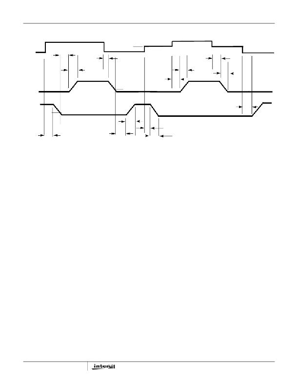
�FIGURE� 1.� TIMING� DIAGRAM�
�Operation� and� Adaptive� Shoot-Through� Protection�
�Designed� for� high� speed� switching,� the� ISL6597� MOSFET�
�driver� controls� both� high-side� and� low-side� N-Channel� FETs�
�from� one� externally� provided� PWM� signal.�
�A� rising� transition� on� PWM� initiates� the� turn-off� of� the� lower�
�MOSFET� (see� Figure� 1).� After� a� short� propagation� delay�
�[t� PDLL� ],� the� lower� gate� begins� to� fall.� Typical� fall� times� [t� FL� ]�
�are� provided� in� the� Electrical� Specifications� .� Adaptive� shoot-�
�through� circuitry� monitors� the� LGATE� voltage� and� turns� on�
�the� upper� gate� following� a� short� delay� time� [t� PDHU� ]� after� the�
�LGATE� voltage� drops� below� ~1V.� The� upper� gate� drive� then�
�begins� to� rise� [t� RU� ]� and� the� upper� MOSFET� turns� on.�
�A� falling� transition� on� PWM� indicates� the� turn-off� of� the� upper�
�MOSFET� and� the� turn-on� of� the� lower� MOSFET.� A� short�
�propagation� delay� [t� PDLU� ]� is� encountered� before� the� upper�
�gate� begins� to� fall� [t� FU� ].� The� adaptive� shoot-through� circuitry�
�monitors� the� UGATE-PHASE� voltage� and� turns� on� the� lower�
�MOSFET� a� short� delay� time,� t� PDHL� ,� after� the� upper�
�MOSFET’s� gate� voltage� drops� below� 1V.� The� lower� gate�
�then� rises� [t� RL� ],� turning� on� the� lower� MOSFET.� These�
�methods� prevent� both� the� lower� and� upper� MOSFETs� from�
�conducting� simultaneously� (shoot-through),� while� adapting�
�the� dead� time� to� the� gate� charge� characteristics� of� the�
�MOSFETs� being� used.�
�This� driver� is� optimized� for� voltage� regulators� with� large� step�
�down� ratio.� The� lower� MOSFET� is� usually� sized� larger�
�compared� to� the� upper� MOSFET� because� the� lower�
�MOSFET� conducts� for� a� longer� time� during� a� switching�
�period.� The� lower� gate� driver� is� therefore� sized� much� larger�
�to� meet� this� application� requirement.� The� 0.4� Ω� on-resistance�
�and� 4A� sink� current� capability� enable� the� lower� gate� driver� to�
�6�
�absorb� the� current� injected� into� the� lower� gate� through� the�
�drain-to-gate� (C� GD� )� capacitor� of� the� lower� MOSFET� and�
�help� prevent� shoot� through� caused� by� the� self� turn-on� of� the�
�lower� MOSFET� due� to� high� dV/dt� of� the� switching� node.�
�Tri-State� PWM� Input�
�A� unique� feature� of� the� ISL6597� is� the� programmable� PWM�
�logic� threshold� set� by� the� control� pin� (VCTRL)� voltage.� The�
�VCTRL� pin� should� connect� to� the� controller� ’s� VCC� so� that�
�the� PWM� logic� thresholds� follow� with� the� VCC� voltage� level.�
�For� applications� using� single� rail� 5V� to� power� up� both�
�controller� and� driver,� this� pin� can� be� tied� to� the� driver� VCC,�
�simplifying� the� trace� routing.�
�The� ISL6597� also� features� the� adaptable� tri-state� PWM�
�input.� Once� the� PWM� signal� enters� the� shutdown� window,�
�either� MOSFET� previously� conducting� is� turned� off.� If� the�
�PWM� signal� remains� within� the� shutdown� window� for� longer�
�than� the� gate� turn-off� propagation� delay� of� the� previously�
�conducting� MOSFET,� the� output� drivers� are� disabled� and�
�both� MOSFET� gates� are� pulled� and� held� low.� The� shutdown�
�state� is� removed� when� the� PWM� signal� moves� outside� the�
�shutdown� window.� The� PWM� rising� and� falling� thresholds�
�outlined� in� the� Electrical� Specifications� determine� when� the�
�lower� and� upper� gates� are� enabled.� During� normal� operation�
�in� a� typical� application,� the� PWM� rise� and� fall� times� through�
�the� shutdown� window� should� not� exceed� either� output’s� turn-�
�off� propagation� delay� plus� the� MOSFET� gate� discharge� time�
�to� ~1V.� Abnormally� long� PWM� signal� transition� times� through�
�the� shutdown� window� will� simply� introduce� additional� dead�
�time� between� turn� off� and� turn� on� of� the� synchronous�
�bridge’s� MOSFETs.� For� optimal� performance,� no� more� than�
�50pF� parasitic� capacitive� load� should� be� present� on� the�
�FN9165.1�
�May� 4,� 2007�
�发布紧急采购,3分钟左右您将得到回复。
相关PDF资料
ISL6605IBZ
IC DRIVER MOSFET DUAL SYNC 8SOIC
ISL6608IR-T
IC MOSFET DRVR SYNC BUCK 8-QFN
ISL6609AIRZ-TK
IC MOSFET DVR SYNC RECT 8-QFN
ISL6610IRZ
IC MOSFET DRVR DUAL SYNC 16-QFN
ISL6612ACBZ
IC DRIVER MOSFET SYNC BUCK 8SOIC
ISL6612BCBZ
IC DRIVER MOSFET SYNC BUCK 8SOIC
ISL6613IR-T
IC MOSFET DRVR SYNC BUCK 10-DFN
ISL6614AIR-T
IC DRIVER DUAL SYNC BUCK 16-QFN
相关代理商/技术参数
ISL6597CRZ-T
功能描述:IC MOSFET DRVR DUAL SYNC 16-QFN RoHS:是 类别:集成电路 (IC) >> PMIC - MOSFET,电桥驱动器 - 外部开关 系列:- 标准包装:50 系列:- 配置:高端 输入类型:非反相 延迟时间:200ns 电流 - 峰:250mA 配置数:1 输出数:1 高端电压 - 最大(自引导启动):600V 电源电压:12 V ~ 20 V 工作温度:-40°C ~ 125°C 安装类型:通孔 封装/外壳:8-DIP(0.300",7.62mm) 供应商设备封装:8-DIP 包装:管件 其它名称:*IR2127
ISL6598DRZ-T
制造商:Intersil Corporation 功能描述:PB-FREE 48LD 7X7 QFN, T&R, GRAPHICS PROCESSOR DIGITAL CONT. - Tape and Reel 制造商:Intersil Corporation 功能描述:IC GRAPHICS PROCESSOR DGTL 制造商:Intersil 功能描述:4 8LD 7X7 GRAPHICS PROCESSOR DIGTL CONT
ISL6605CB
功能描述:IC MOSFET DRVR SYNC BUCK 8-SOIC RoHS:否 类别:集成电路 (IC) >> PMIC - MOSFET,电桥驱动器 - 外部开关 系列:- 标准包装:50 系列:- 配置:低端 输入类型:非反相 延迟时间:40ns 电流 - 峰:9A 配置数:1 输出数:1 高端电压 - 最大(自引导启动):- 电源电压:4.5 V ~ 35 V 工作温度:-40°C ~ 125°C 安装类型:表面贴装 封装/外壳:TO-263-6,D²Pak(5 引线+接片),TO-263BA 供应商设备封装:TO-263 包装:管件
ISL6605CB-T
功能描述:IC MOSFET DRVR SYNC BUCK 8-SOIC RoHS:否 类别:集成电路 (IC) >> PMIC - MOSFET,电桥驱动器 - 外部开关 系列:- 标准包装:50 系列:- 配置:低端 输入类型:非反相 延迟时间:40ns 电流 - 峰:9A 配置数:1 输出数:1 高端电压 - 最大(自引导启动):- 电源电压:4.5 V ~ 35 V 工作温度:-40°C ~ 125°C 安装类型:表面贴装 封装/外壳:TO-263-6,D²Pak(5 引线+接片),TO-263BA 供应商设备封装:TO-263 包装:管件
ISL6605CB-TS2495
制造商:Rochester Electronics LLC 功能描述: 制造商:Intersil Corporation 功能描述:4 A HALF BRDG BASED MOSFET DRIVER, 8 Pin Plastic SOP
ISL6605CBZ
功能描述:功率驱动器IC VER OF ISL6605CB RoHS:否 制造商:Micrel 产品:MOSFET Gate Drivers 类型:Low Cost High or Low Side MOSFET Driver 上升时间: 下降时间: 电源电压-最大:30 V 电源电压-最小:2.75 V 电源电流: 最大功率耗散: 最大工作温度:+ 85 C 安装风格:SMD/SMT 封装 / 箱体:SOIC-8 封装:Tube
ISL6605CBZ
制造商:Intersil Corporation 功能描述:MOSFET Driver IC
ISL6605CBZA
功能描述:IC MOSFET DRVR SYNC BUCK 8-SOIC RoHS:是 类别:集成电路 (IC) >> PMIC - MOSFET,电桥驱动器 - 外部开关 系列:- 标准包装:6,000 系列:*